|
Kyocera Memorabilia
Company: Kyocera Corporation
Based: Kyoto, Japan Founded: 1959 as Kyoto Ceramic Company, Limited Founder: Kazuo Inamori Specialty: World's largest maker of ceramic integrated circuit packages. Leading designer & Manufacturer of advanced materials for the electronics industry including fine ceramic components and semiconductor carrier packages, fiber optic components, solar cells, cell phones, LCD & LED displays, business printers, medical & automotive electronic devices, digital cameras, computer equipment, gaming devices, and wireless networks. Designed and manufactured the TRS-80 Model 100 laptop computer. Introduced one of the earliest smartphones, and earliest mobile phones with built-in camera. |
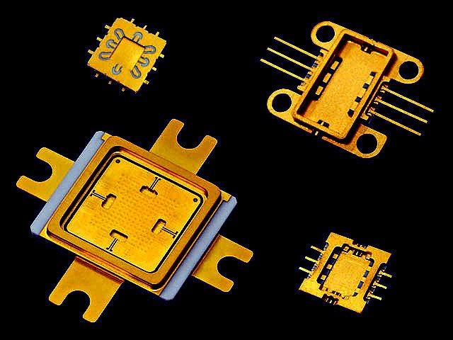
kyocera Ceramic Packages used in Automotive Electronics
|
Kyocera LCC Ceramic & Gold Chip Packaging (Early 2000's)
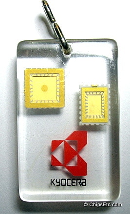
Item #964
This Lucite keychain from Kyocera features two examples of their Multi-layered LCC (lead-less chip carrier) ceramic & gold IC packaging technology used for large-scale integrated circuits that require a low-profile package, such as in a mobile phone.
Kyocera's long history of being the leader in the chip packaging industry began in the mid 1960s. Kyocera's first customer in their expansion into the growing U.S semiconductor market was with Fairchild Semiconductor. Kyocera soon became Fairchild's biggest supplier of Cerdips (ceramic dual in-line packages).
As Fairchild engineers & executives left to form new start ups, many choose Kyocera to continue to supply them with ceramic packages which greatly expanded Kyocera's customer base. (Fairchild spin-off companies include Intel, Intersil, Signetics, AMD, Cirrus Logic, Cypress, National Semiconductor, LSI, PMC-Sierra, Rheem Semiconductor, Chips & Technologies, Atmel, Cadence, Linear Technology, Altera, SanDisk, Computer Microtechnology, Synaptics, Synertek, VLSI Technology, Wafer Scale Integration, Xilinx, Zilog, & others).
In 1971, during the recession, Kyocera would acquire Fairchild's failing semiconductor manufacturing plant located in San Diego CA., and another nearby plant from Honeywell Ceramics, which enabled the company to keep up with their new found U.S. growth. Another 300,000 sq/ft computer assembly plant in San Diego was purchased from Honeywell in 1975. These San Diego plants became the base for Kyocera's new International manufacturing division. By the mid 1980's, Kyocera would control 70 percent of the worlds market for ceramic chip packaging.
In Feb. 2001, Kyocera introduced their $400 Model 6035 "Smartphone", which was the first to combine a cell phone with a Palm handheld computer, and one of the earliest Smartphones to hit the U.S. market.
Keychain purchased in Kyoto Japan in the early 2000's, measures 1 1/2 inches long X 1 inch wide and 3/8 inches thick.
Kyocera LCC Ceramic & Gold Chip Packaging
Items # 1033 & 1034
This Lucite keychain from Kyocera features more examples of their cermaic chip package technologies.
The Multi-layered LCC (lead-less chip carrier) ceramic & gold IC packag upper left corner was used for large-scale integrated circuits that require a low-profile package, such as in a mobile cell phones.
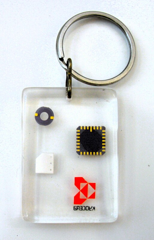
Back of the Kycoera Substrate keychain
|
Kyocera manufactures a wide variety of standard ceramic packages for the semiconductor industry, including:
|
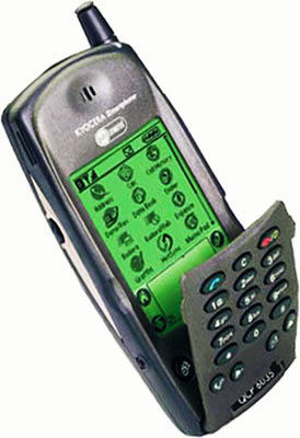
Kyocera model 6035, one fo the first SmartPhones (2001)
|
|