 Lear Siegler Memorabilia Company: Lear Siegler Inc. (LSI)
Based: Los Angeles, Ca. USA Founded: 1961 as merger between the Siegler Corporation & Lear Avionics Inc. Founder: John G. Brooks & William Lear Specialty: Developed numerous Aviation & Aerospace technologies including: inertial guidance systems, "hands off" landing systems, the telemetry & navigational instrumentation for the Apollo Moon missions, and the flight controls for the Lockheed L-1011 commercial aircraft. |
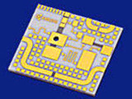 A "Thin Film" gold & ceramic substrate |
Lear Siegler Thin Film Substrate Lapel Stick Pin (1995)
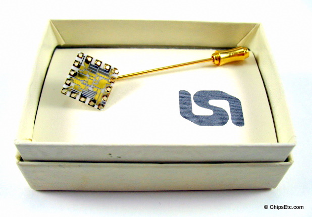
Item #079
Lear Siegler, Inc. (LSI) was a leader in aircraft & aerospace avionics, controls, instruments and navigation systems in the 1960's and 70's.
Notable innovations include inertial guidance systems, "hands off" landing systems, the telemetry and navigational instrumentation for the Apollo moon missions, and the flight controls for the Lockheed l-1011 commercial aircraft.
Lear Siegler also made the ADM series of computer terminals popular in the late 1970's. Lear Siegler was acquired by EG&G defense contractors in 2002.
This is a 16 lead Substrate with Gold plated traces, mounted to a gold plated stickpin. This item is in it's original LSI gift box with information card.
Lear Siegler Thin Film Substrate Tie Tack (1995)
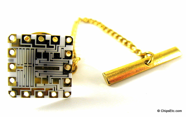
Item #573
This is a 16 lead, gold and ceramic, thin film substrate manufactured by Lear Siegler, made into a gold plated tie tack.
Item comes with an information sheet, and a LSI logo gift box.
Item comes with an information sheet, and a LSI logo gift box.
|
|
 Tie Tack in LSI gift box 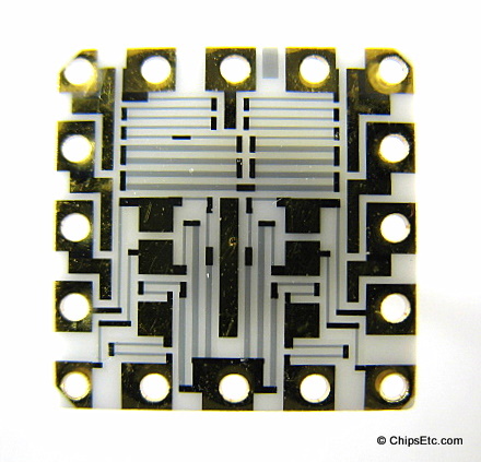 Close-up of the LSI thin film substrate |
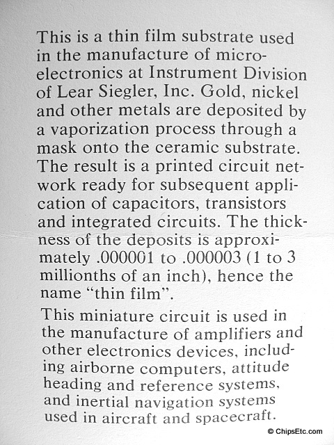 Information card from Lear Siegler |
This is a thin film substrate used in the manufacture of microelectronics at Instrument Division of Lear Siegler, Inc. Gold, nickel and other metals are deposited by a vaporization process through a mask onto a ceramic substrate.
The result is a printed circuit network ready for subsequent application of capacitors, transistors and integrated circuits. The thickness of the deposits is approximately .000001 to .000003 (1 to 3 millionth of an inch), hence the name "thin film". This miniature circuit is used in the manufacture of amplifiers and electronic devices, including airborne computers, attitude heading and reference systems, and inertial navigation systems in aircraft and spacecraft. |