 IBM Memorabilia
|

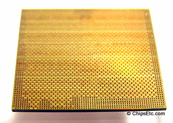
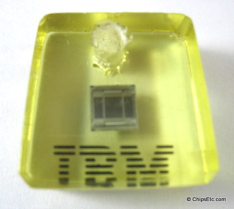
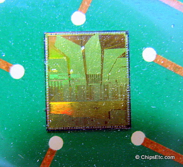
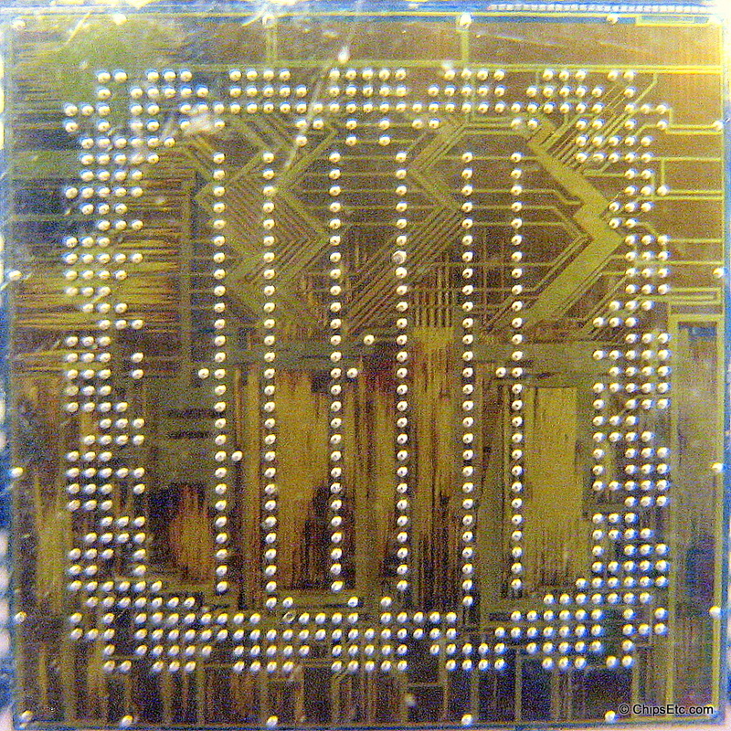
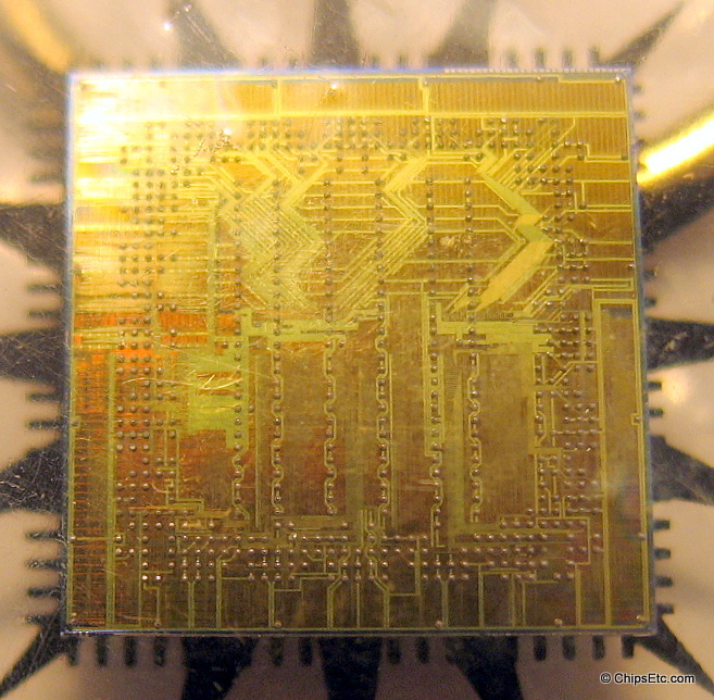
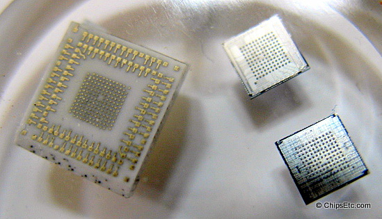
An IBM MLC multi-logic chip carrier (1983)
|
IBM SLT (Solid Logic Technology) Chip Paperweight (1964)
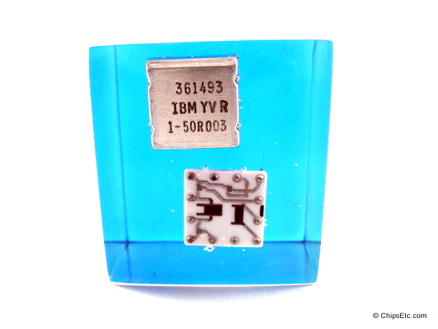
Item #171
An IBM 12-pin IBM SLT solid logic chip & it's cover, encased in blue lucite.
IBM SLD (Solid Logic Dense) Logic Chip (1965)

Item #168
IBM's SLT and SLD were hybrid technologies in which transistors and other components were placed on a ceramic substrate.
MST was the first IBM monolithic integrated circuit technology (multiple circuits on one silicon chip and arranged on a ceramic substrate).
SLT and SLD circuits were used in the IBM System 360 mainframe computers and other IBM peripheral equipment during the mid 1960's.
MST was the first IBM monolithic integrated circuit technology (multiple circuits on one silicon chip and arranged on a ceramic substrate).
SLT and SLD circuits were used in the IBM System 360 mainframe computers and other IBM peripheral equipment during the mid 1960's.
IBM MST (Monolithic Systems Technology) Logic Chip (1968)

Item #169
IBM's MST (Monolithic Systems Technology) logic chips were used in later System 360s such as the Model 85, and all System 370's during the late 1960's and 70's.
Some MST modules used multiple integrated circuits on one ceramic substrate.
Some MST modules used multiple integrated circuits on one ceramic substrate.
IBM MST Logic Chip Paperweight (1968)

Item #170
Another type of IBM MST logic chip with cover encased in blue Lucite.
IBM MST Logic chip (1968)
 sold
sold
An IBM MST logic chip embedded in clear Lucite.
Item measures 1.5" W x 2" H.
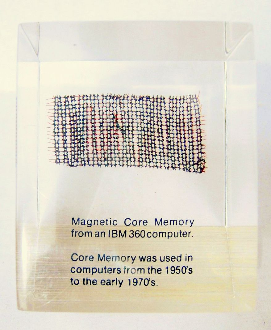
IBM 360 Computer Magnetic Core Memory (early 1970s)
Sold
This Lucite paperweight has an embedded piece of magnetic core memory from an IBM 360 mainframe computer.
Reads "Core memory was used in computers from the 1950's to the early 1970's."
Reads "Core memory was used in computers from the 1950's to the early 1970's."

IBM 360 Computer Magnetic Core Memory
IBM Silicon Paperweight from East Fishkill FAB (late 1970s)

Item #261
This Paperweight has a sample of a silicon ribbon used in IBM's chip manufacturing facility in East Fishkill, NJ.
In 1993 IBM announced that they would be phasing out mass manufacturing of computer chips at it's East Fishkill, New York Fabrication plant (FAB), and would instead use the plant exclusively for making packaging components that hold the silicon chips.
About Silicon Wafers
In 1993 IBM announced that they would be phasing out mass manufacturing of computer chips at it's East Fishkill, New York Fabrication plant (FAB), and would instead use the plant exclusively for making packaging components that hold the silicon chips.
About Silicon Wafers
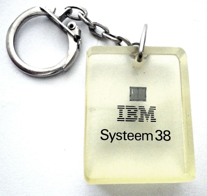
IBM System 38 Server Computer Chip (1978)
Sold
Lucite key chain featuring an IBM System 38 Minicomputer / Server Computer chip.
IBM sold an estimated 20,000 System 38 Computers during the first five years since the computer's first introduction.
IBM sold an estimated 20,000 System 38 Computers during the first five years since the computer's first introduction.
IBM 4300 General Systems Division 32k & 64k Bit Memory Chips (1979)
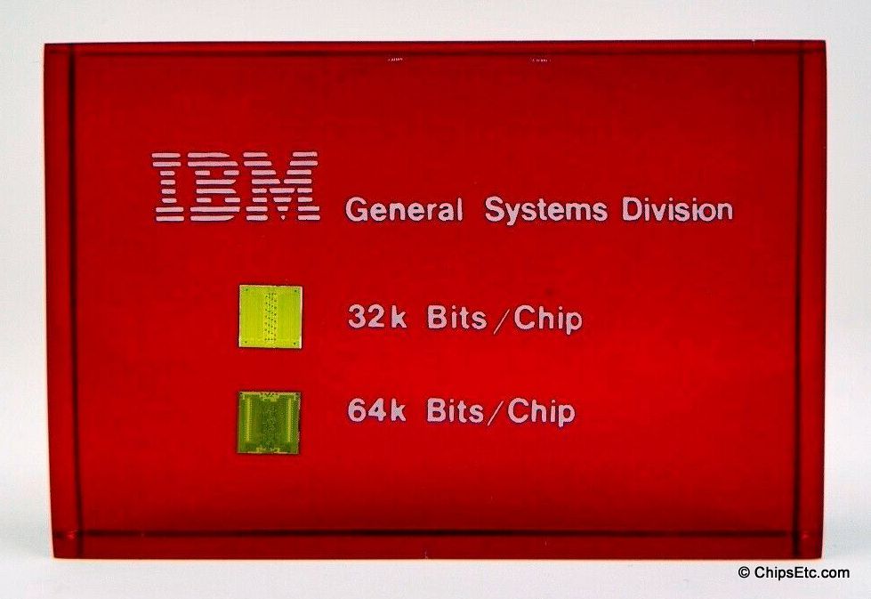
Item #1007
In 1979, IBM introduced the IBM 4300 series computer system with Large Scale Integration (LSI) logic and solid-state memory based on it's new advanced 64k bit chip.
IBM paperweight has the 32k & 64k Bits memory chips embedded inside clear Lucite with a red background. Reads "IBM General Systems Division".
IBM paperweight has the 32k & 64k Bits memory chips embedded inside clear Lucite with a red background. Reads "IBM General Systems Division".
|
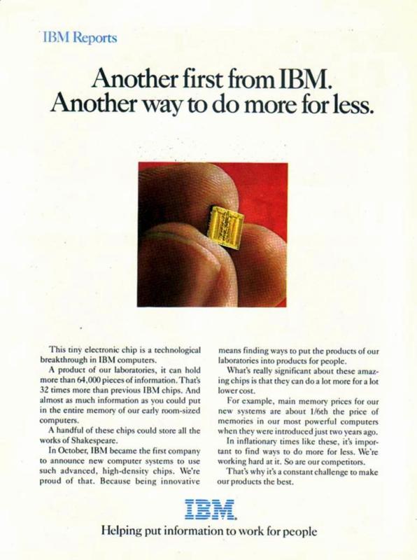
 IBM Silicon Computer Chip Ad (1980) |
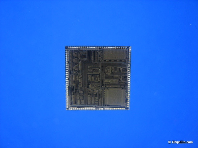
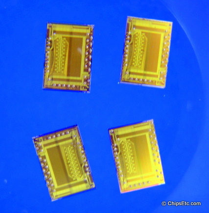
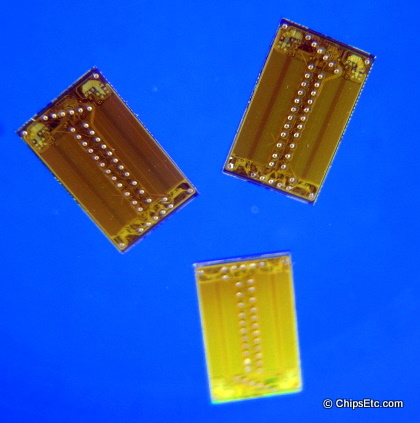
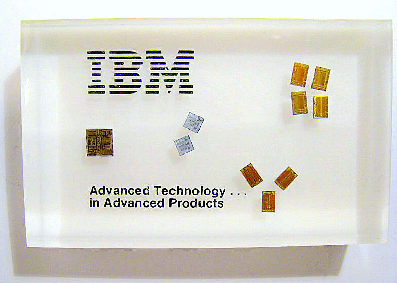
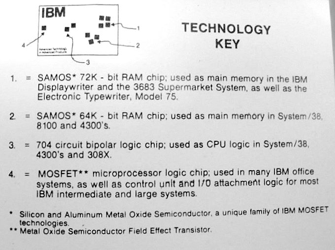
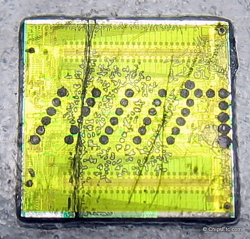
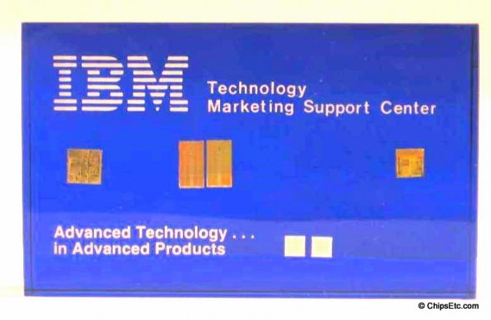
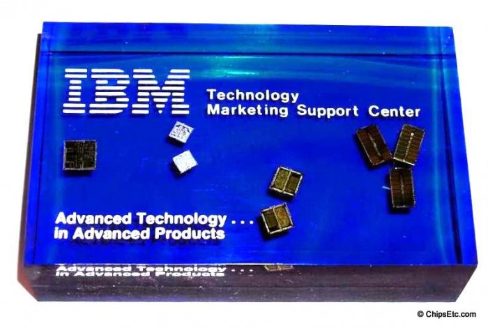
IBM Advanced Technology Paperweight (1979)
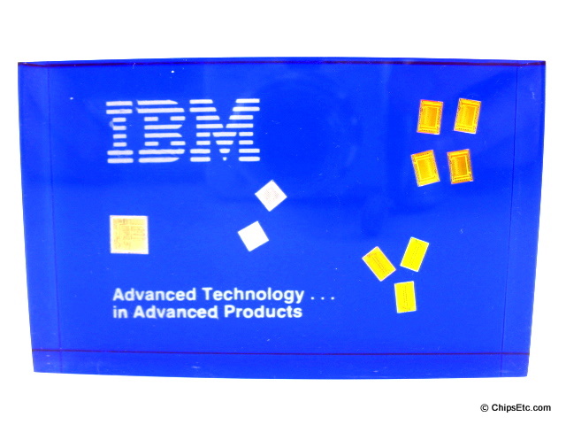
Item #479
IBM Chip Technology paperweight, has four different types of chips embedded in clear Lucite with a blue background.
Actual IBM Chips embedded include: SAMOS 72K and SAMOS 64K RAM chips, the 704 circuit bipolar logic chip, and MOSFET microprocessor logic chip.
Paperweight reads "Advanced Technology...In Advanced Products" on front.
Measures 4" X 2.5" X 1".
Actual IBM Chips embedded include: SAMOS 72K and SAMOS 64K RAM chips, the 704 circuit bipolar logic chip, and MOSFET microprocessor logic chip.
Paperweight reads "Advanced Technology...In Advanced Products" on front.
Measures 4" X 2.5" X 1".


IBM Advanced Technology SAMOS Paperweight (1979)
Sold
Clear Lucite IBM Advanced Technology Paperweight featuring IBM SAMOS (silicon and aluminum metal oxide semiconductor) integrated circuit technology from the late 1970's.
Paperweight has four different types of chips embedded inside. Actual IBM Chips embedded include: SAMOS 72K and SAMOS 64K RAM chips, the 704 circuit bipolar logic chip, and MOSFET microprocessor logic chip.
Paperweight reads "Advanced Technology...In Advanced Products" on front.
Measures 4" X 2.5" X 1"


IBM 64K Memory Chip Die (1978)
Item #754
This is a loose IBM 64K FET Memory chip Die.
The IBM 64K memory chip was developed at IBM's General Technology Division laboratory (Burlington Vermont) and was manufactured at Burlington and IBM's facility in Sindelfingen Germany.
The IBM 64K memory chip was developed at IBM's General Technology Division laboratory (Burlington Vermont) and was manufactured at Burlington and IBM's facility in Sindelfingen Germany.
IBM Advanced Technology SAMOS Paperweight (1979)

Sold
IBM Chip Technology paperweight, has four different types of chips embedded in clear Lucite with red background.
Actual IBM Chips embedded include: SAMOS 72K and SAMOS 64K RAM chips, the 704 circuit bipolar logic chip, and MOSFET microprocessor logic chip.
Paperweight reads "Advanced Technology...In Advanced Products" on front.
Measures 4" X 2.5" X 1".
Actual IBM Chips embedded include: SAMOS 72K and SAMOS 64K RAM chips, the 704 circuit bipolar logic chip, and MOSFET microprocessor logic chip.
Paperweight reads "Advanced Technology...In Advanced Products" on front.
Measures 4" X 2.5" X 1".
IBM Advanced Technology Paperweight (1979)
Sold
IBM Technology Marketing Support Center paperweight, has four different types of chips embedded in clear Lucite with a blue background.
Actual IBM Chips embedded include: SAMOS 72K and SAMOS 64K RAM chips, the 704 circuit bipolar logic chip, and MOSFET microprocessor logic chip.
Paperweight reads "Advanced Technology...In Advanced Products" on front.
Measures 4" X 2.5" X 1"
Actual IBM Chips embedded include: SAMOS 72K and SAMOS 64K RAM chips, the 704 circuit bipolar logic chip, and MOSFET microprocessor logic chip.
Paperweight reads "Advanced Technology...In Advanced Products" on front.
Measures 4" X 2.5" X 1"
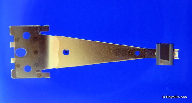
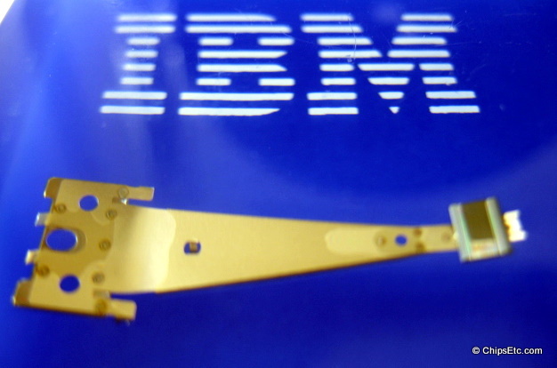
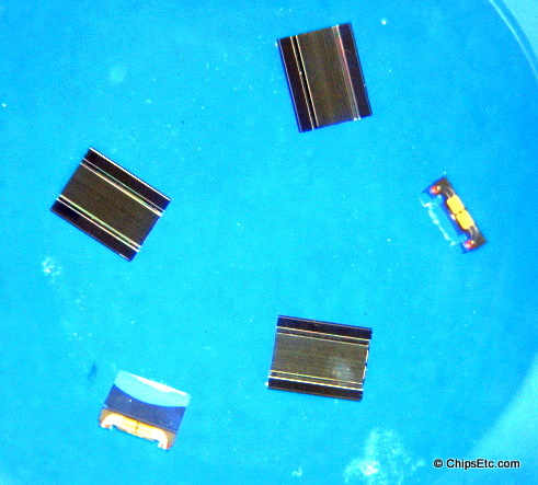
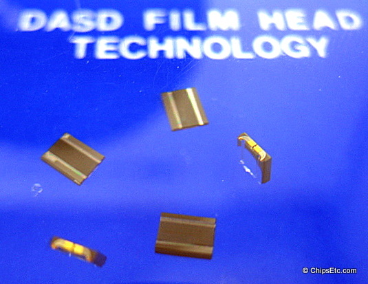
IBM 3370 DASD Film Head Advanced Technology (1979)
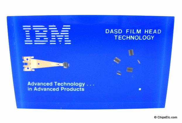
Item #494
The IBM 3370 Direct Access Storage Device that was released in 1979 introduced thin-film head technology to large disk
files. The IBM 3370 was an advanced 571.3MB fixed-media
disk storage for use with the IBM 4331 and 4341 processors and the IBM System/38 midrange
computer.
Work on thin-film disk drive head technology was started in IBM’s Thomas J. Watson Research Center in Yorktown Heights, N.Y. in the late-1960s.
IBM clear Lucite paperweight with blue background has embedded chips & head assembly for the DASD (direct access storage device) Thin-film Head Technology.
Measures 4" x 2 1/2 " x 1".
IBM Advanced Technology Paperweight (1979)
Item #426
IBM Technology Marketing Support Center paperweight, has four different types of chips embedded in Lucite.
Actual IBM Chips embedded include: SAMOS 72K and SAMOS 64K RAM chips, the 704 circuit bipolar logic chip, and MOSFET microprocessor logic chip.
Paperweight reads "Advanced Technology...In Advanced Products" on front.
Measures 4" X 2.5" X 1".
Actual IBM Chips embedded include: SAMOS 72K and SAMOS 64K RAM chips, the 704 circuit bipolar logic chip, and MOSFET microprocessor logic chip.
Paperweight reads "Advanced Technology...In Advanced Products" on front.
Measures 4" X 2.5" X 1".
IBM Computer Chip Keychain (1970s)
Item #434
An unknown IBM computer chip encased in Lucite with IBM logo.
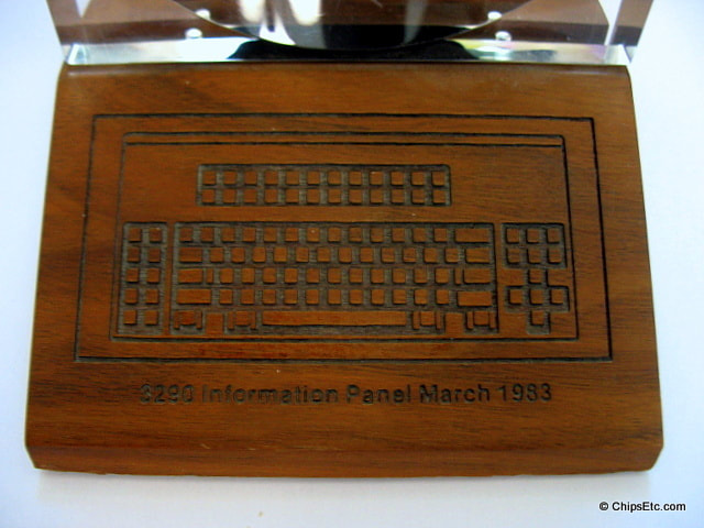
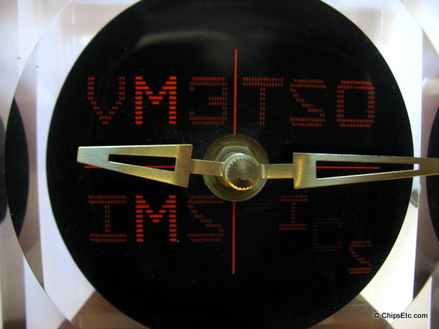
IBM 3290 Information Panel Monochrome Display Paperweight (1983)
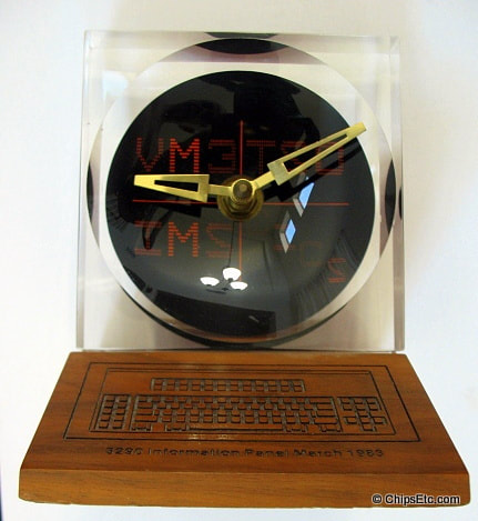
Item #1002
Rare 1980s desk clock which was a promotion for the 3290 plasma display panel released in March of 1983.
The original 3290 monitor was a 19" monochrome display that featured orange text on a black background. It was able to show up to four IBM 3270 terminal sessions at the same time.
1" thick Lucite with circular recess with embedded clock face; keyboard is made from a laser cut piece of hardwood. Clock hands move and are made of brass.
Measures 4.25" wide x 5" tall.

IBM / Intel 386 Button (1986)
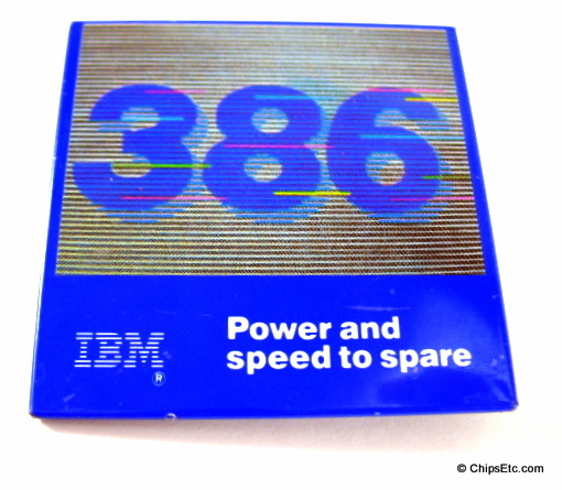
Item #452
The Intel 386 was a 32-bit Microprocessor introduced by Intel in 1985. The first versions had 275,000 transistors.
The 386 was for a time only available from Intel, since Andy Grove, Intel's CEO at the time, made the decision not to encourage other manufacturers to produce the processor as second sources. This decision was ultimately crucial to Intel's success in the market.The 386 was the first significant microprocessor to be single-sourced. Single-sourcing the 386 allowed Intel greater control over its development and substantially greater profits in later years. Production of the 386 lasted until it's end in 2007.
The 386 was for a time only available from Intel, since Andy Grove, Intel's CEO at the time, made the decision not to encourage other manufacturers to produce the processor as second sources. This decision was ultimately crucial to Intel's success in the market.The 386 was the first significant microprocessor to be single-sourced. Single-sourcing the 386 allowed Intel greater control over its development and substantially greater profits in later years. Production of the 386 lasted until it's end in 2007.
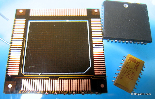
IBM Systems Technology Division Paperweight (1988)
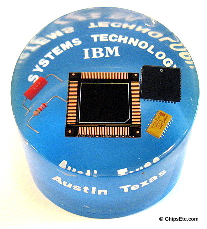
Item #798
This acrylic paperweight was made for their Systems Technology Division in Austin Texas
It features various electronic components and processors, including an Intel 8042 microcontroller used in IBM PC motherboards as a keyboard interface chip, an IBM processor bare substrate, capacitors, and a surface mount resistor.
Paperweight is clear with blue background.
From the IBM Engineer who created these pieces:
This memento has quite a history. Back in the 80's I was part of the Systems Technology Division in IBM Building 045 on Burnet Road in Austin, Texas. Our lab director called some of the development folks to his conference room and asked that we think of a way of providing a memento for the development team on site. He asked for something "nice" that could be placed on desks and wanted at least 800 of them. Since I was a materials engineer I volunteered to get the mementos made using an open cast acrylic resin with local product embedded in the casting. When I went to the local trophy companies their cost per item was way too high. Then I made a mistake!! I volunteered to personally make them. I went to a local supplier of resins and purchased a drum of acrylic resin and some catalyst. Other engineers gathered parts that could be embedded.
Before I could start making them our safety and environmental health shut me down. I wouldn't be allowed to do the work on site because of odor and possible fire hazard concerns. Ouch! I contacted a friend who was also a vendor to IBM and he had a large space available to do the work. I had my materials dropped at his location. Now, I needed hands to help me. No one volunteered except my wife. So, we made the molds, mixed the resin, made the text labels, cured the resin and did the final polishing. 800 almost did us in.
At the end of this venture I had spent >$800 on materials and had a heck of a time getting reimbursed since this was such a stealth operation. However, the lab director was pleased and he passed out the mementos to staff. I was reimbursed but as a "bonus" for getting the job done....no expense account would have been approved.
IBM 1 MEG Computer Memory Chip - National Boyscout Jamboree (1989)

Item #083 (#962 similar)
This IBM 1 megabyte DRAM memory chip would have been the same type of chip used in RAM memory modules put into IBM's popular PS/2 line of home computers and for upgrading some previous IBM PC models.
This pinback button with IBM 1 Meg sticker was given out to Boy Scouts at the 1989 Scout Jamboree which was held at Fort A.P. Hill, Virginia, the very popular IBM booth at the Merit Badge Midway reported 4,000 visitors and 290 Scouts completed the Computers merit badge at the event.
This pinback button with IBM 1 Meg sticker was given out to Boy Scouts at the 1989 Scout Jamboree which was held at Fort A.P. Hill, Virginia, the very popular IBM booth at the Merit Badge Midway reported 4,000 visitors and 290 Scouts completed the Computers merit badge at the event.

Boy scout merit badge for Electronics (1972)
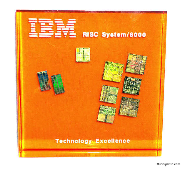
IBM PowerPC RISC System/6000 Computer Chips (1990)
Sold
RISC System/6000, or RS/6000 for short, is a family of RISC and Unix based servers, workstations and supercomputers made by IBM in the 1990's.
The RS/6000 family replaced the IBM RT computer platform in February 1990 and was the first computer line to see the use of IBM's POWER and PowerPC based microprocessors.
The Apple Macintosh would make use of the PowerPC microprocessor in 1992. RS/6000 was renamed eServer pSeries in October 2000.
This Lucite Paperweight has nine computer chips embedded inside including IBM memory chips and processor chips. Top of paperweight is clear and the background is orange.
Measures 4" x 4".
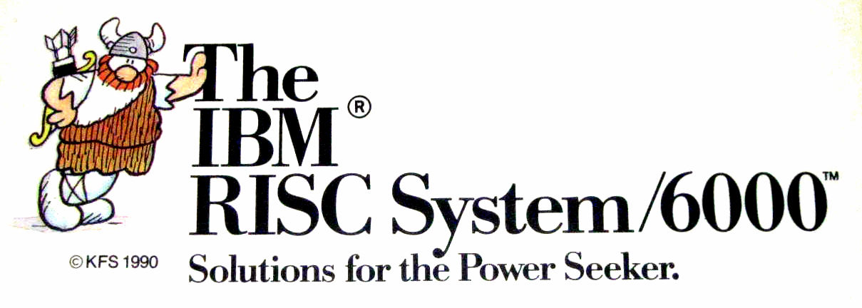
IBM RISC System 6000 Ad (1990)
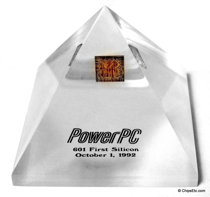
IBM / Motorola PowerPC 601 CPU First Silicon (1992)
Sold
In October 1991 at the Microprocessor Forum in San Francisco, IBM and Motorola outline a four year road map of PowerPC processors, starting with a low-cost desktop processor, and culminating in a high performance processor for servers and workstations. A month later IBM announced the PowerPC 601 microprocessor. Exactly one year later At the 1992 Microprocessor Forum, IBM and Motorola formally announce the beginning of production of PowerPC 601 microprocessors, in 50 MHz and 66 MHz versions.
PowerPC stands for "Power Performance Chip", and incorporates an integer unit, a floating-point unit, and 32 MB cache. IBM produces the processor using 0.6-micron CMOS technology, with 2.8 million transistors per chip.
PowerPC stands for "Power Performance Chip", and incorporates an integer unit, a floating-point unit, and 32 MB cache. IBM produces the processor using 0.6-micron CMOS technology, with 2.8 million transistors per chip.
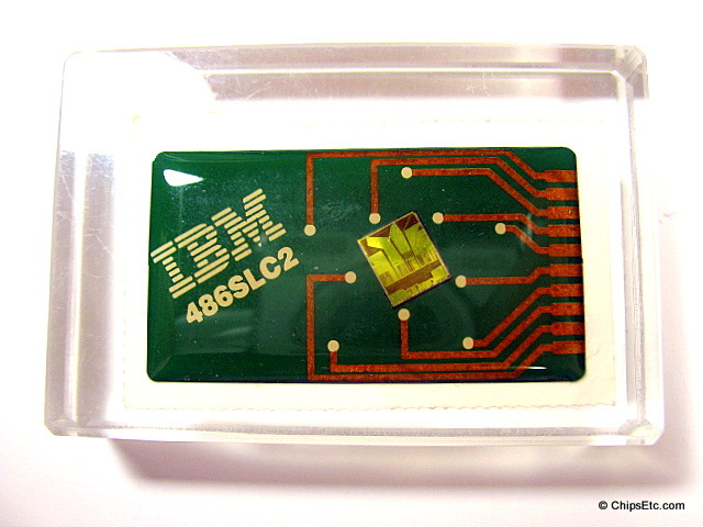
IBM 486SLC2 386 to 486 Upgrade Processor Chip (1992)

Item #894
This trade-show promotional button contains a sample IBM 486 SLC2 processor chip embedded inside.
The IBM 486SLC2 was a clock-doubled version of the IBM 486SLC processor, and used the same instruction set as the 486SLC. It was an IBM developed derivative of Intel's 386SX chip and used the same pin configuration as the 386SX.
This 16-bit processor with 16KB internal cache was first introduced in 1992 as a 40MHz performance upgrade for IBM's 20MHz PS/2 model 56 & 57 386SX / 386SLC based desktop computers.
Cyrix and Intel also competed with IBM by offering their own versions of 386 to 486 processor upgrade chips.
50/25 & 66/33MHz versions of the 486SLC2 processors could later be found in IBM's Thinkpad 500 & 720 models of notebook computers in 1993, and were touted in reviews as being "Rocket-Fast".
IBM would also offer a clock-tripled version of the 486SLC2, called the 486SLC3. It ran at speeds of 60/20, 75/25 and 100/33MHz, dependent on the computers clock speed. The 486SLC3 was the industry's first clock-tripled processor.
Soft plastic button has unused adhesive backing. Comes with clear Lucite block for displaying.
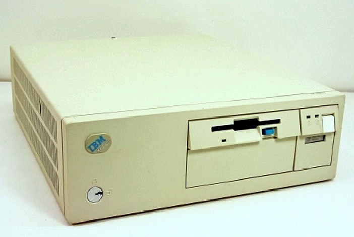
An IBM 486SLC2 powered Model 56 PS/2 Desktop Computer (1993)
IBM PowerPC Chip Keychain (1993)
Item #790 & 793
This Lucite keychain from IBM features an actual PowerPC 601 processor chip.
New, sealed in original packaging.
New, sealed in original packaging.
IBM PowerPC Timeline
|
|
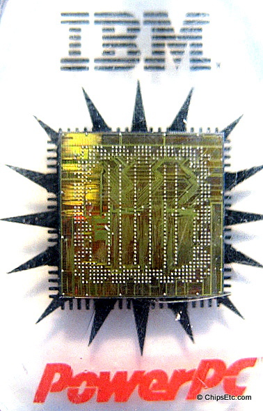
Apple / IBM PowerPC 601 CPU Chip Button (1993)

Sold
The IBM PowerPC 601 chip was the first version of a RISC processor developed jointly between IBM Microelectronics and Motorola.
The PowerPC 601 was the first generation of microprocessors to support the basic 32-bit PowerPC instruction set. The 601 processor ran at speeds of 55-80Mhz. IBM was the sole manufacturer of the 601 and microprocessors in its Burlington, Vermont & East Fishkill, New York production facilities. The 601 was manufactured using IBM's CMOS-4s process.
First launched in IBM systems in the fall of 1993, it was marketed by IBM as the PPC601 and by Motorola as the MPC601. It operated at speeds ranging from 50 to 80 MHz. It was fabricated using a 0.6 µm CMOS process with four levels of aluminum interconnect. The die was 121 mm² large and contained 2.8 million transistors.
The 601 has a 32 kB unified L1 cache, a capacity that was considered large at the time for an on-chip cache. Thanks partly to the large cache it was considered a high performance processor in its segment, outperforming the competing Intel Pentium. The PowerPC 601 was used in the first Power Macintosh computers from Apple, and in a variety of RS/6000 workstations and SMP servers from IBM and Groupe Bull.
Stick-on promotional button has a real power PC chip encased inside enamel for viewing.
SSA Serial Storage Architecture Computer Chip (1995)
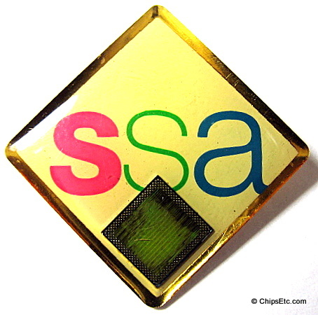
Item #743
This is an enamel pinback with an IBM SSA (Serial Storage Architecture) computer chip embedded inside.
An Engineer at IBM, Ian Judd, first created the SSA protocol back in 1990 to replace SCSI (small computer system interface) used to link hard disk drives to mainframe server computers.
IBM's first product implementation using SSA was on hard drive storage units for the IBM RS/6000 RISC UNIX Servers.
SSA offered increased speed over SCSI, as well as improved fault tolerance and data security, offered full-duplex, bi-directional communications between the computer and storage drives.
SSA protocol circuitry was built on a single integrated CMOS chip that would be used with the disk controller cards.

Close-up of the SSA computer chip
IBM AS/400 PowerPC 64-bit RISC CPU (1995)

This Lucite keychain contains an actual IBM 64-bit RISC CPU, known as Cobra or A10. It was the first PowerPC-AS processor made for the AS/400 server computer systems.
The PowerPC-AS CPU ran at 50-77 MHz. and had 4.7 million transistors. Die size was 14.6 mm by 14.6 mm. It was manufactured by IBM using their 0.5 µm CMOS (four-layer-metal) process.
The PowerPC-AS CPU ran at 50-77 MHz. and had 4.7 million transistors. Die size was 14.6 mm by 14.6 mm. It was manufactured by IBM using their 0.5 µm CMOS (four-layer-metal) process.
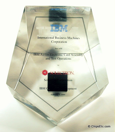
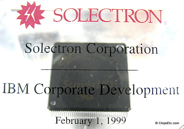
IBM Austin Electronics Card Assembly & Solectron w/ Chip (1999)
 Item #841
This large Lucite paperweight commemorates the sale of IBM's Austin Texas Electronics Card Assembly & Test operations to Solectron Corporation on Feburary 1, 1999. Solectron was a contract electronic manufacturer based in Milpitas CA.
As part of the sale agreement, Solectron would provide PCB assembly services to IBM for three years, and become the exclusive provider of PCBs for IBM "Thinkpad" notebook computer models. Solectron would also lease IBM's 405,000 sq. ft. manufacturing facility in Austin for three years, and would offer employment to 1,300 IBM employees at the manufacturing center.
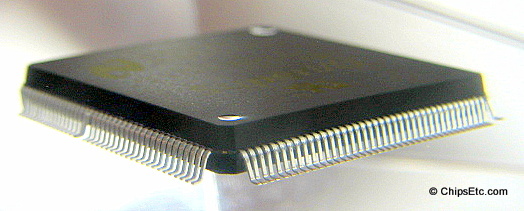
Interestingly, embedded inside is not an IBM chip, but a National Semiconductor Super I/O chip in Quad flat packaging (QFP).
As part of the sale agreement, Solectron would provide PCB assembly services to IBM for three years, and become the exclusive provider of PCBs for IBM "Thinkpad" notebook computer models. Solectron would also lease IBM's 405,000 sq. ft. manufacturing facility in Austin for three years, and would offer employment to 1,300 IBM employees at the manufacturing center.
Interestingly, embedded inside is not an IBM chip, but a National Semiconductor Super I/O chip in Quad flat packaging (QFP).
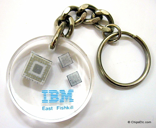
IBM Multi-layer Ceramic TCM IC Packaging Keychain (1990)
Item #869 & 870
This Lucite keychain features another example of IBM's Advanced Integrated Circuit packaging that were used in their ES/9000 (Models 820 and 900) mainframe computers.
Embedded inside is a section of MLC (Multi-Layer Ceramic) substrate with gold pads that would have been part of a larger array of chips composing a TCM (Thermal Conduction Module), and two accompanying IBM processor chips.
Multi-layer Ceramic packages have been produced at IBM's East Fishkill, NY Advanced Packaging Technology facility since 1963 up until 2015 when the plant was sold to Global Foundries.
Only readable identifier on these chips is "7040B".


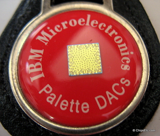
IBM Palette DAC PC video display chip (early to mid 1990s)
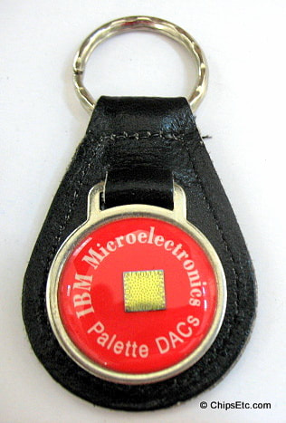
Item #1003
This leather keychain with metal framed fob has a IBM Microelectronic's Palette DAC (Digital to Analog converter) chip.
The Palette DAC chip was used in IPC graphics display controllers for storing the color palette data, and for generating the analog signals that were sent to the IBM PC's color VGA monitor.
The Palette DAC chip was used in IPC graphics display controllers for storing the color palette data, and for generating the analog signals that were sent to the IBM PC's color VGA monitor.


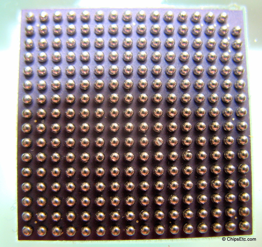
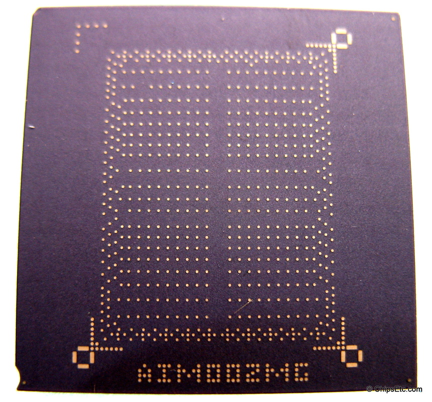
IBM Ceramic Chip Packaging Paperweight (2002)
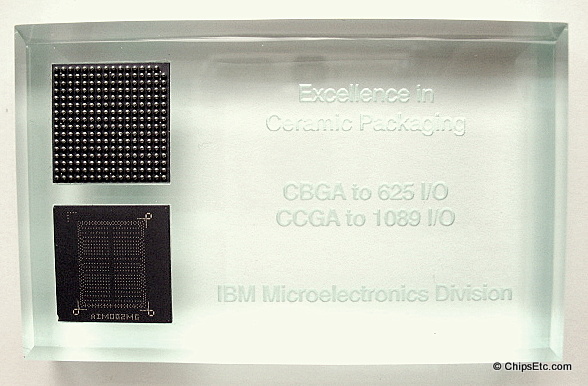
Item #820
This glass paperweight features examples of IBM Microelectronics Division's ceramic packaging.
Attach to the top of the glass is a Ceramic Ball Grid Array (CBGA) with 625 interconnects, as well as a Ceramic Column Grid Array (CCGA) with 1089 Interconnects.
Ceramic packaging is used for applications requiring higher board-level reliability. CBGA packages are used for applications requiring very high-density interconnections - they use high-temperature solder columns instead of high-temperature balls.
Reads "Excellence in Ceramic Packaging" - engraved on the bottom of glass. Measures 4" x 2.5" x .75"

ibm.com OneXperience website launch (2004)
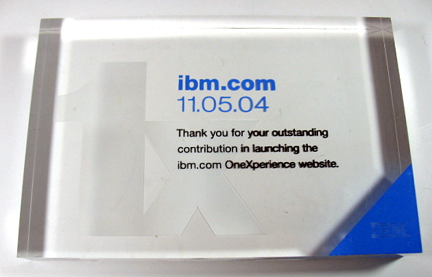 Item #845
This IBM Lucite paperweight commemorates the launch of the new ibm.com website (called OneXperience) on November 5, 2004.
IBM OneXperience made significant steps in making it easier for customers to access IBM's products, services, and business expertise by launching a major redesign of www.ibm.com - the first in four years.
IBM OneXperience made significant steps in making it easier for customers to access IBM's products, services, and business expertise by launching a major redesign of www.ibm.com - the first in four years.
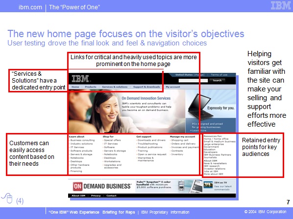
IBM presentation for new IBM.com website (2004)
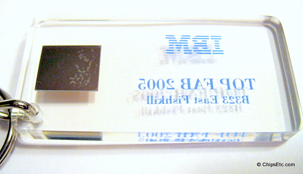
IBM Fab 323 B323 East Fishkill Chip Keychain (2005)
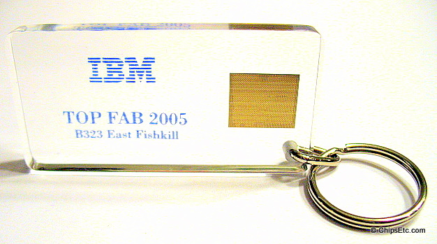
Item #601
IBM's Fab Building 323 (B323) was IBM's first 300mm semiconductor Fab. Located in East. Fishkill, NY. it was opened in 2003 with a $2.5 billion price tag.
This keychain features an IBM CMOS chip embedded in Lucite. It was given to IBM employees at Fab 323 to celebrate the Fab winning the 2005 Semiconductor International Top Fab Award.
OAK BROOK, Ill., 12/01/05 PRNewswire
Semiconductor International has announced its 2005 Top Fab of the Year Award winner as IBM Building 323, East Fishkill, N.Y. The 2005 winner is featured in the December issue of the magazine. "IBM's Fab 323 exemplifies the state-of-the-art in global semiconductor manufacturing," noted Peter Singer, Editor-in-Chief of Semiconductor International. "It is a fully automated 300 mm fab where a diverse set of complex products are produced with the latest process technologies, such as strained silicon. We were particularly impressed with the fab's 'first-time right' track record."