Vintage CPU Computer Chips
and Hardware
Intel 4004 - The First Microprocessor (1976)
Item #001
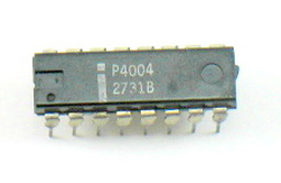
The Intel 4004 was the very first commercial Microprocessor, introduced in 1971.
The 4004 had 2300 transistors & was manufactured using 10um technology, the size of the Die was 3mm x 4mm (1/8" x 1/6") and operated at between 500 & 740kHZ.
This is an Intel P4004 microprocessor in Plastic DIP packaging from 1976.
New & unused.
The 4004 had 2300 transistors & was manufactured using 10um technology, the size of the Die was 3mm x 4mm (1/8" x 1/6") and operated at between 500 & 740kHZ.
This is an Intel P4004 microprocessor in Plastic DIP packaging from 1976.
New & unused.
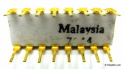
Intel White Ceramic & Gold DIP Chip (early 1970s)
Item #766
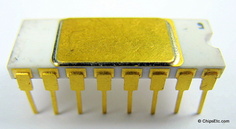
An unmarked Intel white ceramic DIP chip with Gold lid and leads, manufactured in Malaysia.
This may be either an early ROM chip or 4004 Microprocessor Chip.
Gift from Intel Corp. Item was featured in the The "Intel - Innovations in Arizona" exhibit at the Arizona Science Center in 2014.
This may be either an early ROM chip or 4004 Microprocessor Chip.
Gift from Intel Corp. Item was featured in the The "Intel - Innovations in Arizona" exhibit at the Arizona Science Center in 2014.
Intel 8080 CPU (mid 1970s)
Item #772
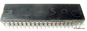
An unmarked Intel 8-bit 8080 test CPU manufactured in the Philippines, in plastic DIP packaging.
Top of chip is hand scribed "SOC".
Gift from Intel Corp. Item was featured in the The "Intel - Innovations in Arizona" exhibit at the Arizona Science Center in 2014.
Top of chip is hand scribed "SOC".
Gift from Intel Corp. Item was featured in the The "Intel - Innovations in Arizona" exhibit at the Arizona Science Center in 2014.
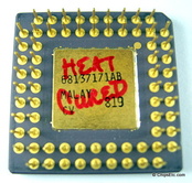
Intel 386 SX 16MHz Microprocessor (1987)
Item #764
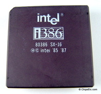
Intel 386 SX 16MHz Microprocessor in PGA packaging (upgrade option). The Intel 386-SX was a low cost version of the 32-bit 80386 processor with a reduced 16-bit data bus.
This unit was used for testing by Intel and is hand marked "heat cured" on the underside.
Gift from Intel Corp. Item was featured in the The "Intel - Innovations in Arizona" exhibit at the Arizona Science Center in 2014.
This unit was used for testing by Intel and is hand marked "heat cured" on the underside.
Gift from Intel Corp. Item was featured in the The "Intel - Innovations in Arizona" exhibit at the Arizona Science Center in 2014.
HP White Ceramic & Gold Processor Chip (1986)

Item #773
An HP Microprocessor in white ceramic DIP packaging with gold leads from a Mid 1980's Electronic Test Analyzer.
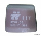
IIT 3C87-33 80387 33MHz Match Co-Processor Chip (1988)
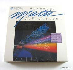
Item #429
This is an IIT 33MHz Math Co-Processor used to upgrade the performance of an 386 computer system for processing intensive math applications (like CAD).
This chip was direct pin and instruction compatible with the Intel 80387 Co-Processor chips but was touted as being 2 to 3 times as fast as similar Intel 80387 Chips and was priced lower as well.
Other competitors to take on Intel in the booming Co-Processor market besides IIT were Cyrix & Weitek.
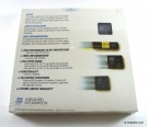
This item is new & sealed in its original retail packaging.
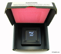
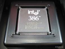
Intel 386SL 20MHz Mobile CPU Engineering Sample (1990)
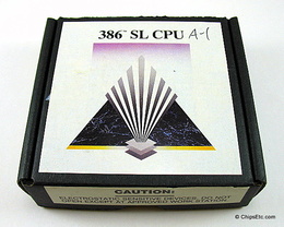
Item #273
The Intel i386SL was introduced as a power efficient version for early laptop computers (Intel 386 Laptop computers first emerged as a portable computing platform in 1990).
This processor offered several power management options, as well as different "sleep" modes to conserve battery power. It also contained support for an external cache of 16 to 64 kb. The extra functions and circuit implementation techniques caused this variant to have over 3 times as many transistors as the i386DX. The i386SL was first available at 20 MHz clock speed, with the 25 MHz model later.
In October 1990, Intel released the 80386SL, which was basically an 855,000 transistor version of the 386SX processor, with cache, bus, and memory controllers, ISA compatibility and power management circuitry. It added a special system management mode (SMM), in which the BIOS could more easily perform power management and other functions without requiring OS support. The 386SL was the first chip specifically made for portable computers.
This was a presentation award given to a select Intel employees who worked on the i386 Processor program. It is hand-marked "A-1" on the box which is for the first version of this chip manufactured by Intel.
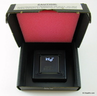
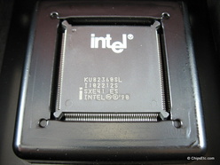
Intel 82360SL Mobile I/O Chip Engineering Sample (1990)
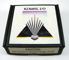
Item #272
The Intel 82360SL Chip was an I/O support chip for the Intel 386SL processor (item shown above) and was used in early laptop computers.
This was a presentation award given to select Intel employees who worked on the i386 Processor program.
This was a presentation award given to select Intel employees who worked on the i386 Processor program.
Motorola 68040 Microprocessor Test Sample (1990)
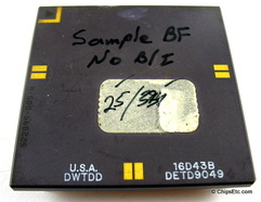
Item #611
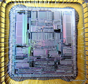
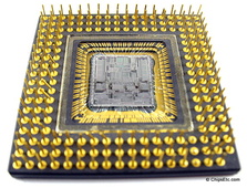
This is a sample Motorola 68040 Microprocessor that features an exposed die without lid and comes in PGA ceramic package with gold wire & pins.
Handwritten markings on top from sample testing; "Sample BF, No B/I, 25/33"
The Motorola 68040 was used in Apple Macintosh Quadra computers.
Intel HD-PQFP Chip Sample (1992)
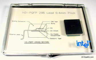
Item #893
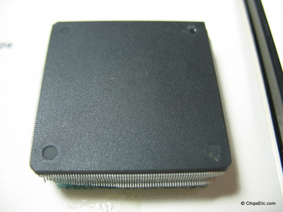
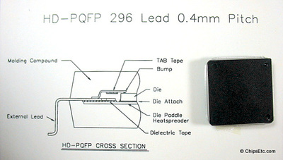
This sample from Intel showcases their 296 lead 0.4mm pitch "HD-PQFP" (high-density plastic quad flat package).
Hinged plastic display case with old Intel logo has a cross-sectional drawing showing the internals of the HD-PQFP package, as well as an unmarked Intel sample chip mounted on foam riser.
Hinged plastic display case with old Intel logo has a cross-sectional drawing showing the internals of the HD-PQFP package, as well as an unmarked Intel sample chip mounted on foam riser.
MIPS / Toshiba R4000 64-bit Engineering Sample CPU (1993)
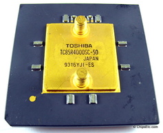
Item #612
This is a Toshiba R4000 "Magnum" (R4000 SC-50) 50 MHz 64-bit CPU that was an Engineering Sample that features a gold lid that has two threaded lugs. It comes in a 447-pin ceramic and gold pin PGA package.
The R4000 RISC microprocessor was developed by MIPS Computer Systems (a fab-less company) and was manufactured by various semiconductor manufacturers including Toshiba.
The R4000 was one of the first 64-bit microprocessors and the first to use MIPS III Instruction set architecture (ISA). This microprocessor had 1,300,000 transistors and was manufactured using 0.8 µm CHMOS technology.
This is the R4000/SC version which had the 1MB secondary cache memory option and was aimed at high-performance desktops and servers.
DEC Alpha 64-bit RISC Microprocessor (1994)
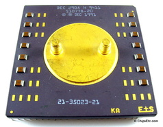
Item #610
This is a 190MHZ version of a DEC Alpha 64-bit RISC microprocessor that was originally used in a Silicon Graphics Workstation.
The DEC Alpha had 1,680,000 transistors. This version has a ceramic PGA with gold-plated top and bottom caps. The top lid has two threaded gold plated lugs.
The DEC Alpha had 1,680,000 transistors. This version has a ceramic PGA with gold-plated top and bottom caps. The top lid has two threaded gold plated lugs.
Intel 486DX2 50MHz CPU (1992)
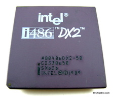
Item #308
The Intel 486 DX2 was introduced in 1992 and was the first Microprocessor to use clock doubling.
This is the 25mhz version that ran at 50mhz.
The 33mhz version of the Intel 486DX2 running at 66mhz was popular with video gamers until the Pentium Processor was introduced in 1993.
This is the 25mhz version that ran at 50mhz.
The 33mhz version of the Intel 486DX2 running at 66mhz was popular with video gamers until the Pentium Processor was introduced in 1993.
Intel 486 Engineering Sample CPU (1989)
Item #748
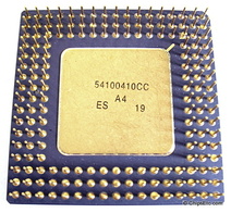
This is an Intel 486 (80486) ceramic CPU that has an unmarked top.
The bottom cap is gold-plated and reads "54100410CC" and is marked "ES" for engineering sample. This CPU was manufactured in Chandler AZ (A4).
The bottom cap is gold-plated and reads "54100410CC" and is marked "ES" for engineering sample. This CPU was manufactured in Chandler AZ (A4).
Intel Pentium Processor Mechanical Sample (1992)
Item #439
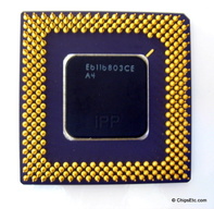
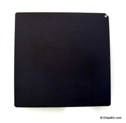
This is an Intel Ceramic Pentium PGA mechanical sample, Marked "IPP" "A4" and "Eb11b803CE" on the back, top is unmarked except for a white dot in the corner to shown Pin 1 location.
Mechanical samples were issued in limited quantities for pre-release for computer systems development by Intel's OEM computer customers.
This chip was manufactured in Chandler AZ (A4).
Mechanical samples were issued in limited quantities for pre-release for computer systems development by Intel's OEM computer customers.
This chip was manufactured in Chandler AZ (A4).
Intel Pentium Mechanical Sample CPU (1992)
Item #338
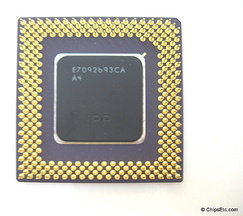
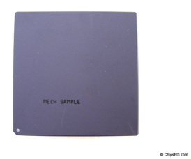
This is an Intel Pentium ceramic 296 pin PGA, with 3,200,000 transistors.
Circuit Size is 0.60 µ, Manufactured around 1992 in Chandler, Arizona (A4).
This CPU is marked "MECH SAMPLE" on top.
Circuit Size is 0.60 µ, Manufactured around 1992 in Chandler, Arizona (A4).
This CPU is marked "MECH SAMPLE" on top.
Intel's First Pentium Processor - Original 60MHz (1993)
Item #303 (#304 & 307 similar)
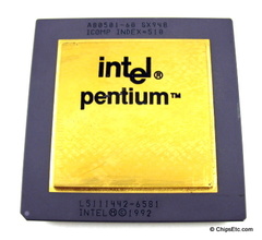
First in Intel's Pentium series of processors was the 60MHz rated CPU, released in 1993.
The Pentium 60MHz was manufactured using 0.8 micron BiCMOS process and contained 3.1 million transistors
This one is a Ceramic PGA with Gold plated Cap and pins.
Marked "A80501-60 SX948".
The Pentium 60MHz was manufactured using 0.8 micron BiCMOS process and contained 3.1 million transistors
This one is a Ceramic PGA with Gold plated Cap and pins.
Marked "A80501-60 SX948".
Intel Pentium 75MHz P54C Processor (1995)
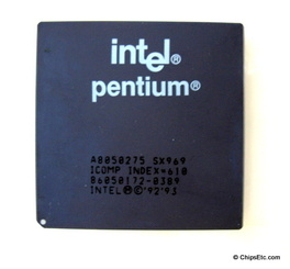
Item #337
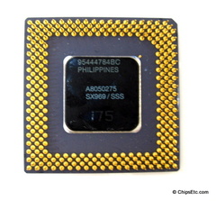
This is a Pentium A80502-75 SX969, 75MHz, C2 stepping, P54C, ceramic PGA 296 pin processor with 3.2 million transistors.
Circuit Size is 0.60 µ and it was manufactured in 1995 in the Philippines.
Circuit Size is 0.60 µ and it was manufactured in 1995 in the Philippines.
Intel Pentium Pro Processor 150 MHz Engineering Sample (1995)
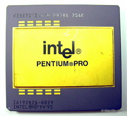
Item #757
This is the original Intel Pentium Pro CPU that was the first to be released to commercial production at a speed offering of 150 MHz. It came in ceramic PGA packaging with gold cap and pins.
The top of the processor has Qspec marking "Q0706" which identifies this an an Intel Engineering Sample. The back lid was un-soldered & discarded during engineering testing by Intel.
The two separate chips that make up this multi-chip processor are now visible: the 256k L2 Cache memory chip, and the 5.5 million transistor CPU chip that Intel fabricated using a 0.50 µm BiCMOS process.
Intel EPROM Programming Module (1984)
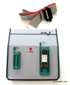
Item #352
In July 1984, using a fab from Ricoh, the company’s first foundry partner, Altera shipped the EP300 device. Its subsequent technology and second-sourcing partnership with Intel Corporation was a major breakthrough that broadly acknowledged the merits of Altera’s approach.
Intel’s wafer technology provided the basis for Altera’s initial revenue ramp in the 1980s. In an ironic twist, Altera, then entering into hyper-growth, bought Intel’s PLD business in 1994.
This is an Intel PLD (Programmable Logic Device) interface module for use with Altera EP1200 & EP300 series reprogrammable devices, it was connected to a development system computer via the module's Serial RS232 connector cable.
Intel SDK-85 8085 Microcomputer System Development Kit (1977)
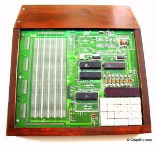
Item #353
In the early years of Microprocessor development, each time Intel introduced a new microprocessor (the Intel 8085 Microprocessor in this case) they would simultaneously offer a System Development Kit (SDK) allowing computer programmers & engineers a way to introduce themselves to the new processor's features and helped third part developers with hardware and software applications.
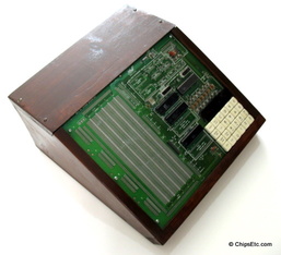
The 8085 kits usually came in component form with a printed circuit board (PCB) that required the owner to assemble and solder. An external 5V/12V power supply unit was required to operate the SDK-85, it was not included with the SDK-85 kit.
The SDK-85 was a complete microcomputer system on a single PCB board including 256 to 512 bytes fo RAM memory and 2k of ROM memory, a 24 key hexadecimal keyboard, a 6 digit LED display, I/O connections and an expansion area allowing memory and I/O expansions as well as hardware experiments.The system used an Intel 8085A (5 for 'first 5 Volt microprocessor') CMOS MPU running at 3.072 MHz. The Intel 8085 microprocessor was designed for use in high-performance applications ranging from controllers to 8-bit minicomputers.
A 2 KB monitor software stored on ROM chip provided the same commands as the SDK-86 board. User could enter and read program results through either the buit-in keyboard/display or using a serial Teletype through the built-in serial TTY interface. A 38 line parallel interface was also available.
This vintage SDK-85 computer was completely assembled back in the 1970's from the original Intel kit components and was nicely mounted in a solid wood case for use by it's builder.
The PCB Board itself Measures 30.5 (W) x 25.7 (D) x 1.3 (H) cm.
Minimum system configuration consisted of the 8085 microprocessor, 8155, 2K RAM, I/O Timer, and
8355 16K ROM & I/O or 8755 16K erasable ROM & I/O .
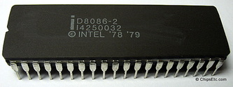
Intel D8086 & other Chips (1970s & 80s)
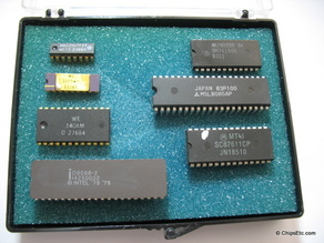
Item #745
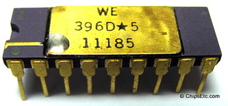
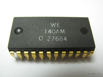
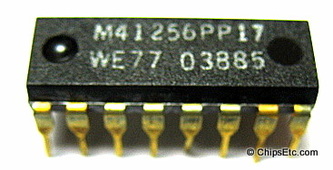
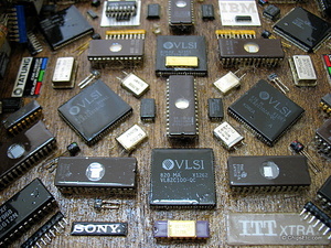
This is a small collection of various computer chips from the 1970's & 80's.
It contains DIP chips from Western Electric, Mitsubishi & Motorola, as well as an Intel D8086 CPU.
It contains DIP chips from Western Electric, Mitsubishi & Motorola, as well as an Intel D8086 CPU.
Motorola MC6800 Educator II Power Supply HEP Kit (1977)
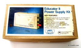
Item #354
Motorola's HEP/MRO Operations group introduced the 8-bit microcomputer system in kit form.
Called the Educator II, the kit contained an NMOS 8-bit MPU (running at 625 kHz), PIA, 128x8-bit static RAM, two TTL 512x4-bit ROM's, and a TTL clock circuit.
Educator II utilized the full instruction set and address modes of the Motorola MC6800 MPU.
This HEP boxed item was the optional power supply kit designed specifically for the Educator II, originally priced at $29.95. This power supply was assembled back in the 1970's from the kit components and is fully functional. Output is 5V d.c. / 1amp / 60 Hz.
Promotional Sample Computer Chip (1980s)
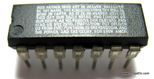
Item #598
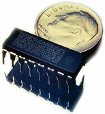
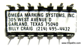
This Unique Integrated Circuit Chip has the the text of the Lord's Prayer printed on it in Micro-Lettering as a Promotional item given out in the 1980's by Omega Marking Systems Inc. of Garland Texas.
Omega Marking, Inc. was founded in 1980 in Garland, Texas located at the heart of Texas's Silicon Corridor. They are a full service marking and coding device contractor dedicated to providing the highest quality marking devices available to the electronic, semiconductor, and pharmaceutical industries.
This chip showcased the quality of this company's marking ability for use on electronic devices and in the semiconductor industry.
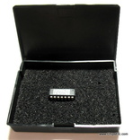
Unknown manufactured 14-lead DIP Chip. New, unused in black plastic case. Underside of chip is labeled with the address of the Omega Marking Systems, Inc., Garland Texas, & Billy Craig.
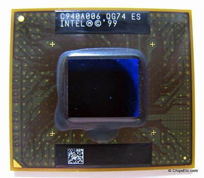
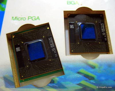
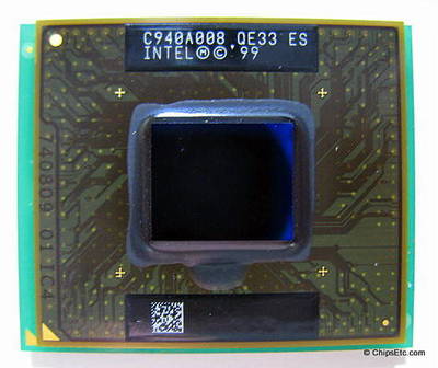
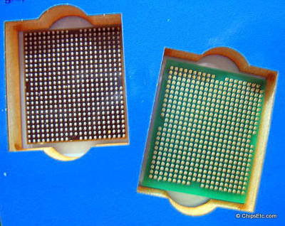
Intel Mobile Pentium III Processor Product Samples (1999)
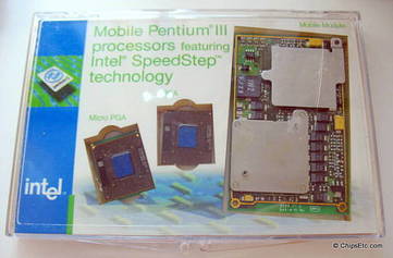
Item #977
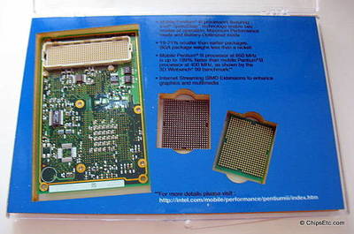
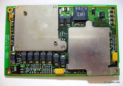
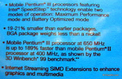
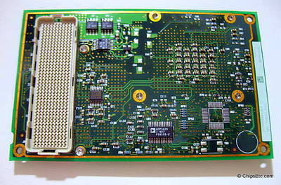
This is a promotional sales display from Intel that has examples of the 3 different Mobile processor products being offered in 1999.
Displayed in a hinged clear plastic case with Intel blue / white cardboard insert that identifies each chip and allows the chips to be viewed from front and back.
Chip examples include the Intel Pentium III processors in both Micro PGA (Pin) and BGA (Ball) packaging, as well as an Intel Pentium III mobile module (composed of the processor, chipset, and L2 cache)
The PGA & BGA Pentium III processors are marked as ES (Engineering sample).
Intel Desktop, Mobile & Server Processor Product Samples (2008)
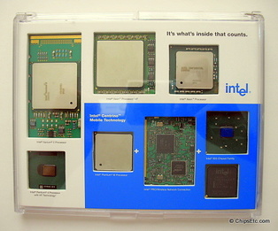
Item #821
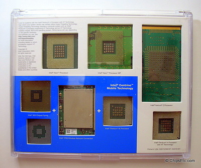
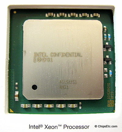
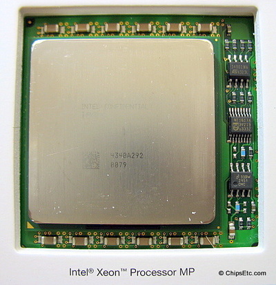
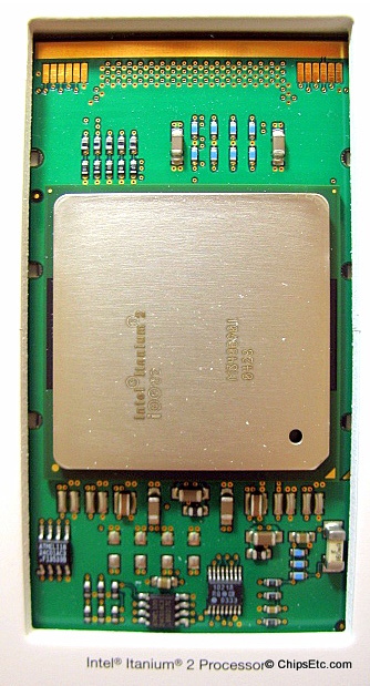
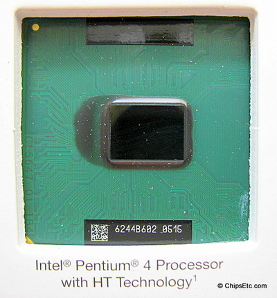
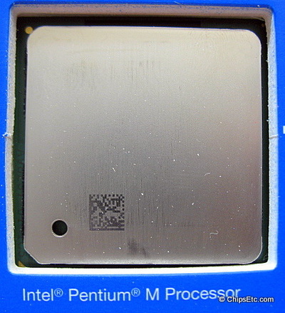
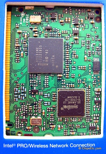
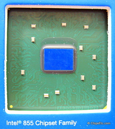
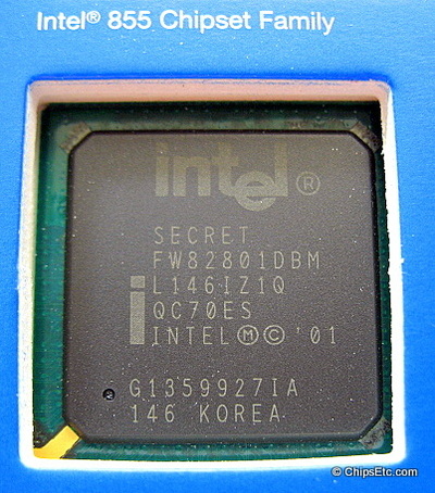
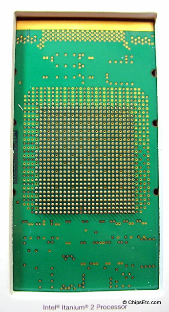
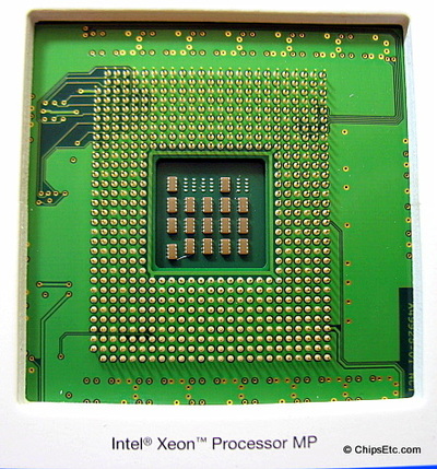
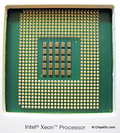
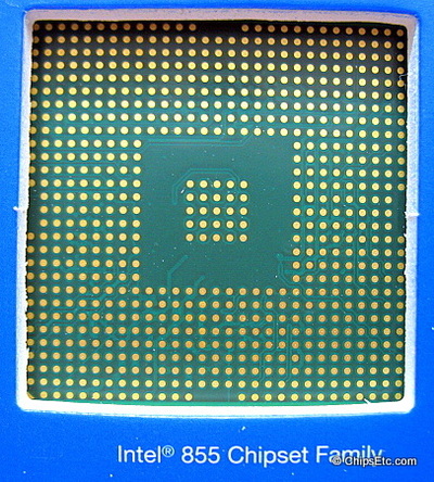
This is a promotional sales display showcasing the 8 different Intel products being offered in 2008 - all nicely displayed in a hinged clear plastic case with Intel blue / white cardboard insert that identifies each chip and allows the chips to be viewed from front and back.
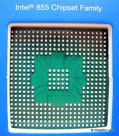
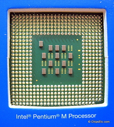
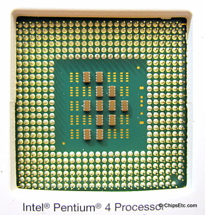
Chips include the Intel Itanium 2, Intel Pentium 4 with Hyper Threading, Intel Xeon MP, Intel Xeon, Intel Centrino Family with Intel Pentium M, Intel Pro Wireless and the Intel 865 chipset.
Many of these are pre-production samples and are marked as ES (Engineering sample), Secret, & Intel Confidential.
Intel ATOM Processor (2008)
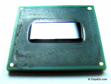
Item #765
An unmarked Intel ATOM Processor in unused BGA (Ball Grid Array) organic substrate packaging.
The Intel ATOM processor was an ultra-low-voltage CPU used in netbook computers, mobile internet devices, and embedded computing applications, manufactured using Intel's 32nm CMOS technology.
Gift from Intel Corp. Item was featured in the The "Intel - Innovations in Arizona" exhibit at the Arizona Science Center in 2014.
Intel Pentium 2.5 GHz Dual Core Processor (2008)
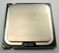
Item #768
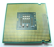
An Intel Pentium Dual Core 2.5 GHz E5200 processor.
This 64-bit Pentium Dual Core processor had two separate dies with each having a single core, contained side by side in a multi-chip module package. Manufactured using Intel's 45nm technology.
This 64-bit Pentium Dual Core processor had two separate dies with each having a single core, contained side by side in a multi-chip module package. Manufactured using Intel's 45nm technology.
Intel Core 920 i7 Processor (2008)
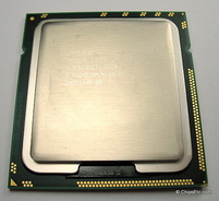
Item #767
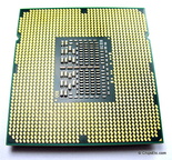
An Intel "920" Core i7 2.66 GHz processor.
This 64-bit Quad core processor was manufactured using Intel's 45nm technology and had 731 million transistors.
This 64-bit Quad core processor was manufactured using Intel's 45nm technology and had 731 million transistors.
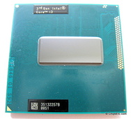
Intel Core i3 Laptop processor (2008)
Item #771
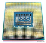
An Intel Core i3 64-bit processor in PGA packaging.
This processor is special laser marked "3rd Gen Intel Core i3".
Gift from Intel Corp. Item was featured in the The "Intel - Innovations in Arizona" exhibit at the Arizona Science Center in 2014.
This processor is special laser marked "3rd Gen Intel Core i3".
Gift from Intel Corp. Item was featured in the The "Intel - Innovations in Arizona" exhibit at the Arizona Science Center in 2014.
