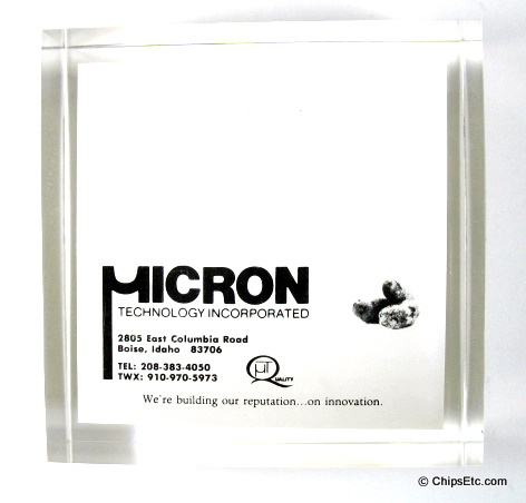
|
Company: Micron Technology, Inc.
Based: Boise, ID. Founded: 1978 Founder: Ward Parkinson, Joe Parkinson, Dennis Wilson & Doug Pitman. Specialty: Manufactures Advanced Semiconductor products including DRAM & Flash memory, CMOS image sensors, semiconductor components, & memory modules for use in leading-edge computing, consumer, networking, server, mobile, & automotive products. World's second largest memory manufacturer behind Samsung. |
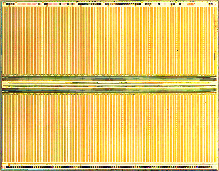
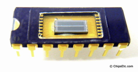
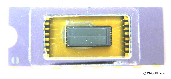
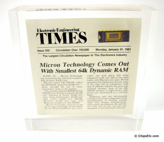
Micron Technology MT4246A 64k DRAM Memory Chip (1983)

Sold
The Micron Technology MT4246A 64-kilobit DRAM chip, introduced in 1983, represents a key technical milestone in the company’s formative years and illustrates the process and design challenges of early dynamic memory development.
Micron Technology, founded in 1978 in Boise, Idaho, was a vertically integrated semiconductor startup focused on the design and fabrication of MOS memory devices.Entering the DRAM memory chip market required rapid mastery of circuit design, lithography, process integration, and yield management—disciplines typically dominated at the time by much larger U.S. and Japanese semiconductor firms.
Micron engineers completed the original 64K DRAM design in 1979, targeting a density that was at the leading edge of commercial computer memory technology. The device employed a classic one-transistor, one-capacitor (1T1C) DRAM cell architecture, requiring precise control of capacitor formation, thin-oxide integrity, and leakage currents to meet retention and refresh specifications. Initial production devices were shipped in 1981, marking Micron’s first successful entry into the commercial DRAM memory chip market and validating its in-house fabrication capability.
The MT4246A revision, completed in 1983, represented the first “shrink” of Micron’s 64K DRAM. This shrink reduced the die area while maintaining the same memory capacity and electrical interface, enabling improved wafer utilization and lower cost per bit. Achieving this shrink required tighter lithographic alignment, refined diffusion and deposition steps, and improved defect density control to preserve acceptable yields. Such process shrinks were critical to economic survival in the DRAM market, where cost reductions often determined competitiveness more than raw performance.
The introduction of the MT4246A was publicly recognized in a January 21, 1983 announcement in Electrical Engineering Times, which described the device as the world’s smallest DRAM at the time. This distinction highlighted Micron’s ability to compete at the process-technology level with far larger manufacturers. The device was packaged in a standard dual in-line package (DIP), consistent with early 1980s system integration practices, and met contemporary JEDEC interface expectations for 64K DRAMs.
The Lucite paperweight associated with the MT4246A serves as a technical artifact commemorating this achievement. Embedded within it is an actual MT4246A DIP device with the intergated circuit package lid removed, exposing the silicon die. The visible die layout provides insight into early DRAM floorplanning, including the regular memory array structure, peripheral sense amplifiers, and row/column decoding circuitry. As a historical and technical object, the MT4246A illustrates how Micron’s early emphasis on process refinement, die shrinks, and manufacturing discipline established the foundation for its long-term role as a leading global supplier of memory semiconductors.


