History of Silicon Wafers
used in the Semiconductor Industry
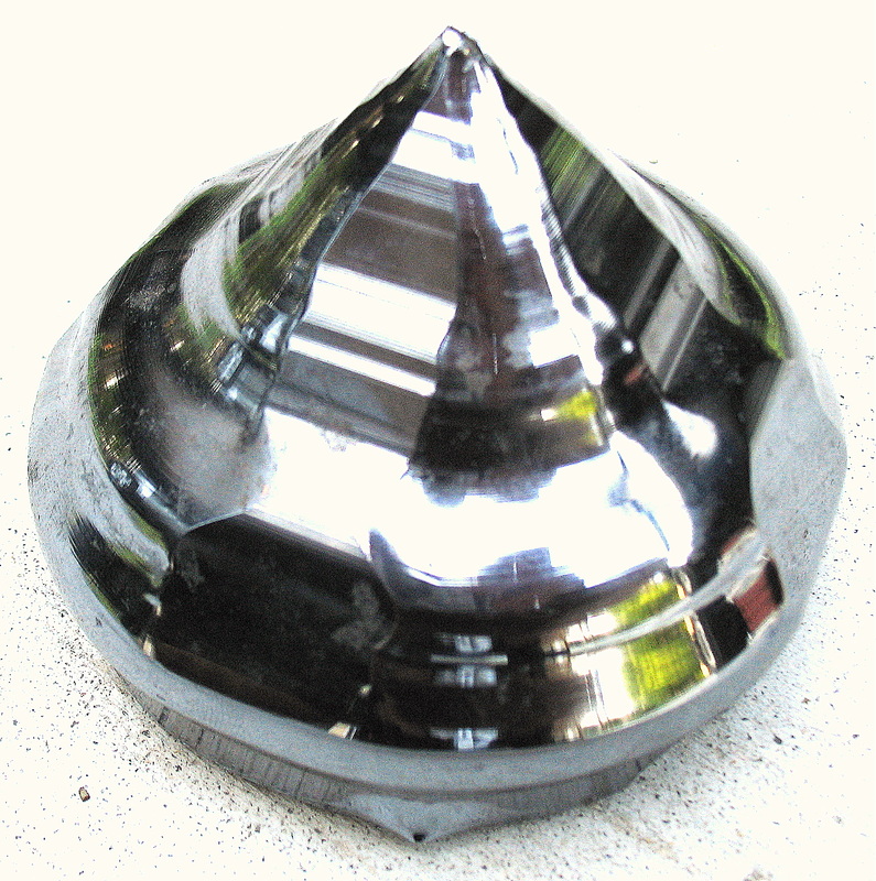
End of a Silicon Ingot
Silicon (Si), a Semiconducting material made from silica, is the fundamental building block of modern integrated circuits, diodes, rectifiers, transistors, and solar cells.
The history of Silicon starts with it's discovery by Jöns Jacob Berzelius, a Swedish chemist, in 1824. For the next 130 years Silicon would not see any major industrial uses.
Fast forward to the late 1940's when companies including RCA & Western Electric are working on creating some of the very first transistors using a different semiconducting material other than Silicon, a material called Germanium (Ge).
However, by the early 1950's Silicon is found to be a much more efficient semiconducting material than Germanium, it raises the power output while lowering operating temperatures. In 1954, Silicon becomes born in the transistor industry when Texas Instruments produces the first commercial silicon transistor. Silicon becomes responsible for enabling the miniaturization of electronics!
Today, most transistors, integrated circuits, memory chips, and even Solar Cells, are still manufactured using Silicon in the form of wafer slices that are sawn from a grown silicon ingot.
Silicon is commercially processed by the reaction of high-purity silica with wood, charcoal, and coal, in an electrically heated arc furnace using carbon electrodes. At temperatures over 1,900 °C (3,450 °F), the carbon reduces the silica to silicon.
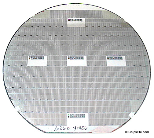
Silicon Semiconductor Wafers - Size & Thickness

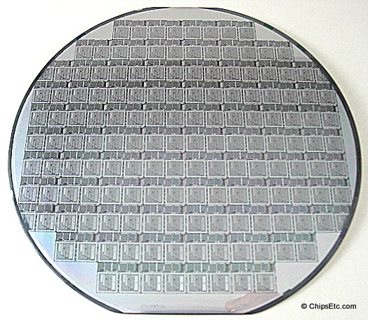
Silicon ingots and wafers in various sizes
The Industry standard Silicon wafer size is currently 300mm (12") in diameter.
A consortium of semiconductor companies including Intel, Samsung, Global Foundries, and TSMC are currently working on the development of the industry's next generation of wafers which will increase their size to 450mm (18") diameter and greatly increase future production yields.
Intel introduced the industry's first fully patterned 450mm wafer at the SEMI Industry Strategy Symposium in January 2013.
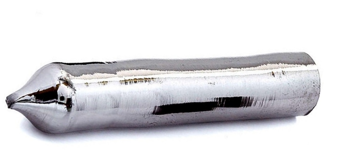
A silicon ingot before being sliced into wafers
Silicon Wafers continue to grow in size
|
Intel Corp. has been at the forefront of developing larger Silicon Wafers for use in manufacturing it's famous CPU's & computer chips.
They started development of their first memory chip products using the industry standard 2" wafers way back in 1969! The first microprocessor, the Intel 4004, was manufactured using 2" silicon wafers starting in 1971. Specifications of Silicon Wafers (1960 to Present): YEAR DIAMETER WAFER THICKNESS 1960 0.9" (23mm) ???? 1960 1" (25mm) ???? 1963 1.1" (28mm) ???? 1969 2" (50 mm) 275 µm 1972 3" (75 mm) 375 µm 1976 4" (100 mm) 525 µm 1981 5" (120, 125 &130 mm) 625 µm 1983 6" (150mm) 675 µm 1992 8" (200mm) 725 µm 2002 12" (300mm) 775 µm ???? 18" (450 mm) ~925 µm |
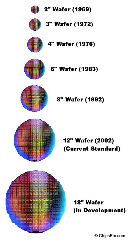
History of Intel Silicon Wafer Sizes
|
Apple, IBM and Intel share Silicon Wafer Development
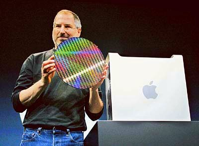
Steve Jobs with a IBM PowerPC wafer (2003)
|
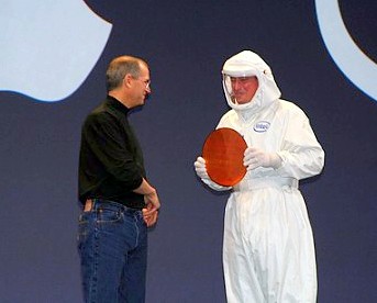
Apple's Steve Jobs and Intel's Paul Otellini with Intel Silicon wafer at MacWorld (2006)
|
How Silicon Wafers are Made - Semiconductor Wafer Fabrication

semiconductor wafer fabrication
Intel shows off the Semiconductor Industry's Future: The 450mm Silicon Wafer
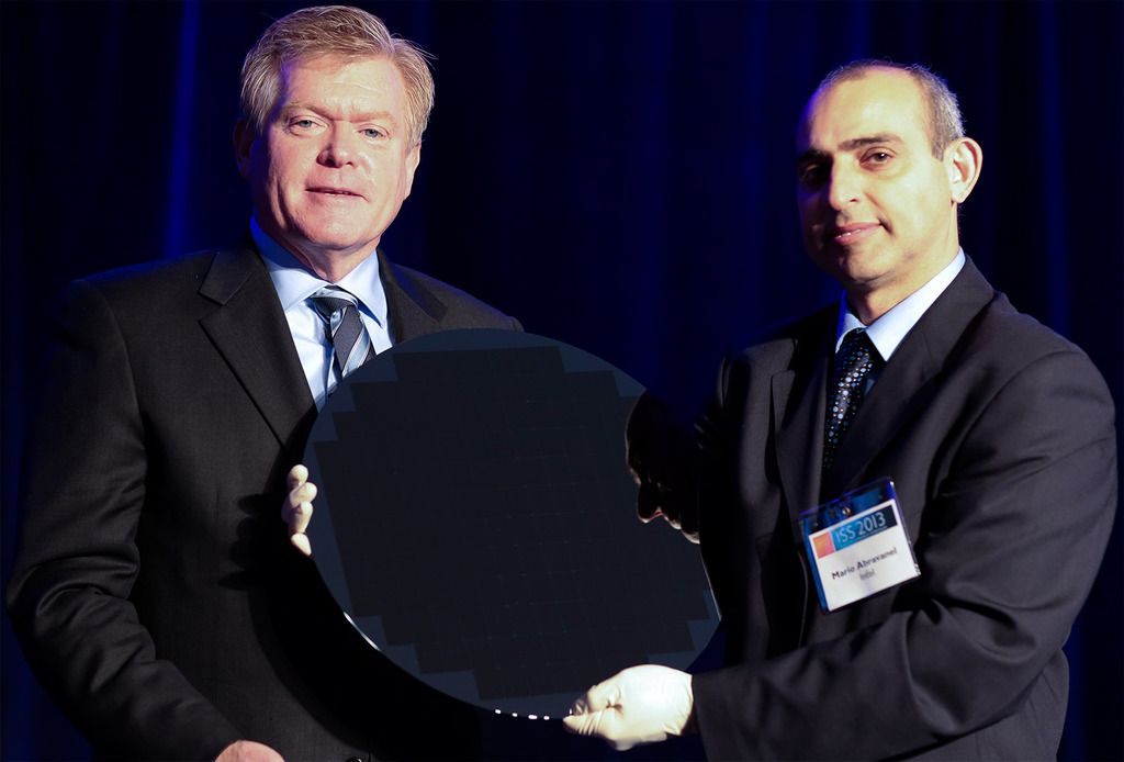
Intel's first developmental 450mm wafer (2013)
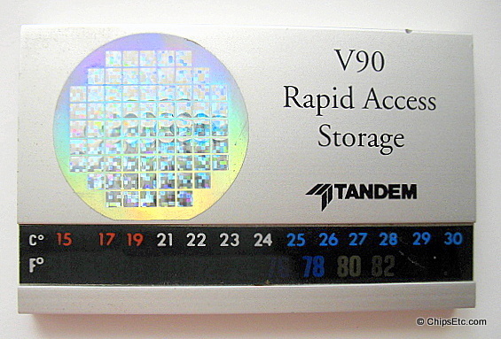
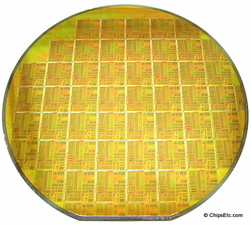
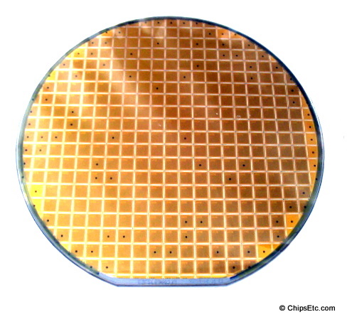
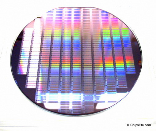
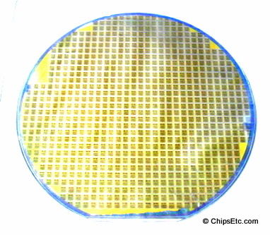
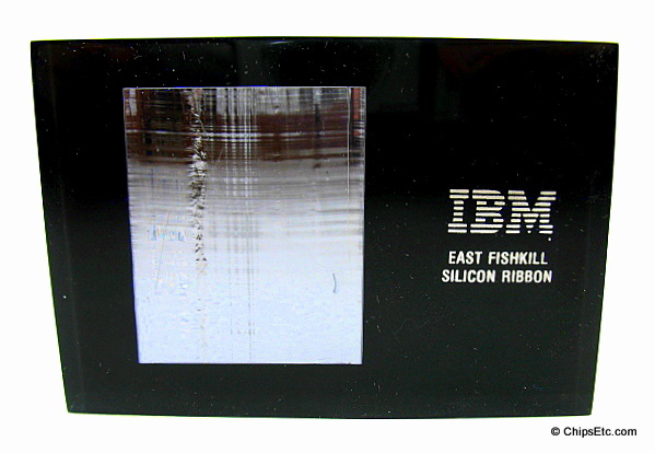
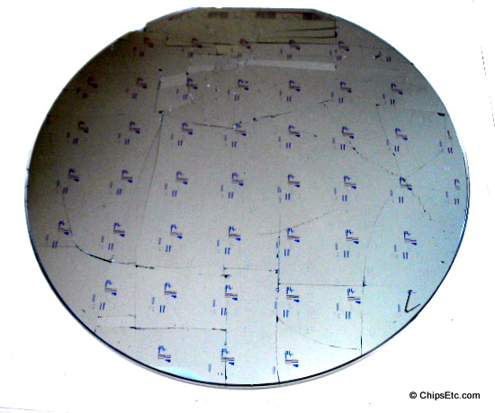
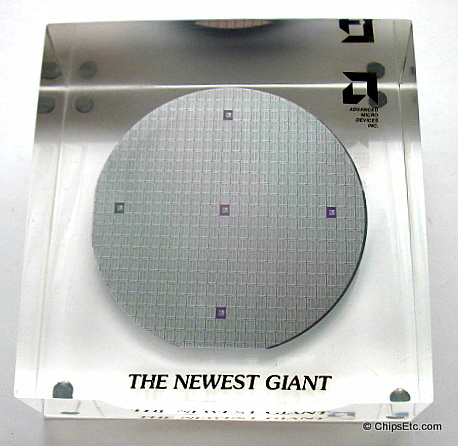
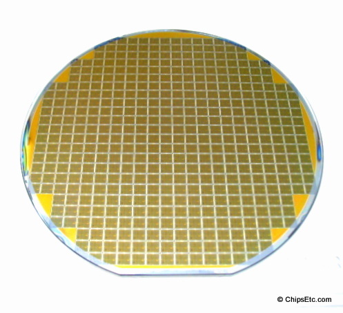
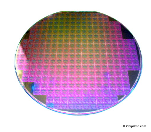
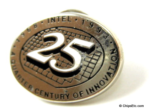
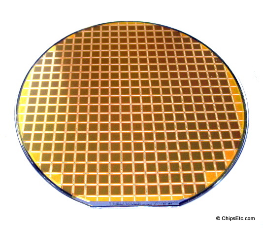
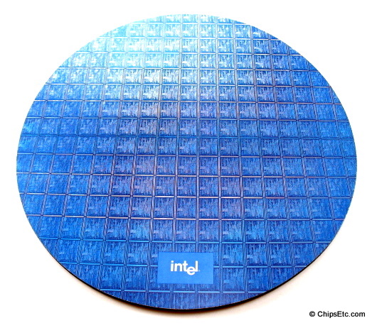
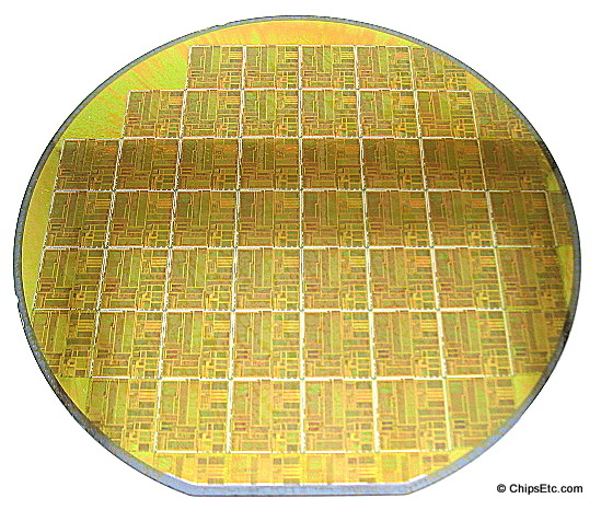
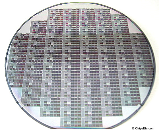
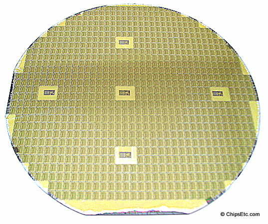
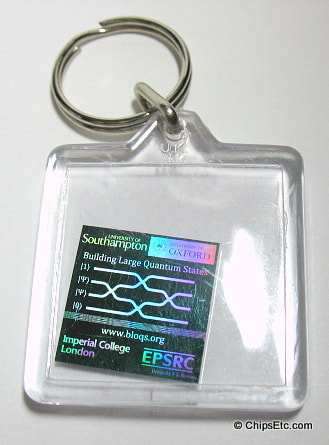
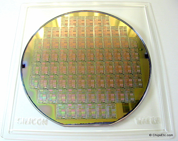
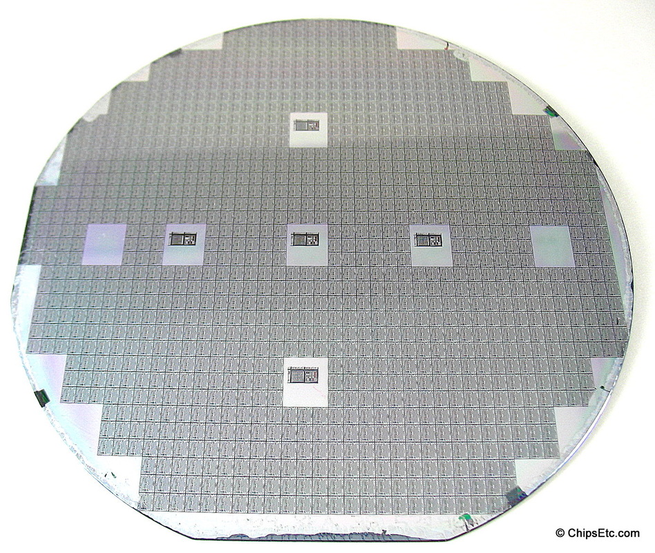
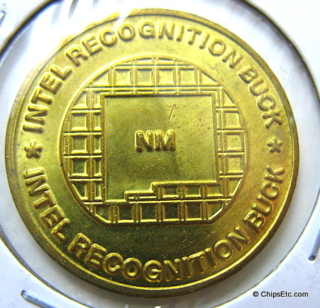
Some Memorabilia with Silicon Wafers